Peter L. Levin
Amida Technology Solutions, Inc.
April 2024
Executive Summary
Amida has developed an innovative solution to enhance the cybersecurity of semiconductor devices, and to incorporate cyber-attack resilience onto the chip itself. Our methodology proactively identifies and mitigates design vulnerabilities. It is based on a graph transform of the RTL, coupled with machine learning, that exposes cybersecurity threats that formal methods will not reveal. This design-for-security-and-trust (DFST) approach determines the location and type of exposure, suggests, and inserts compact surveillance instruments, and can produce hardened devices that detect and potentially remediate attacks. When these hardened components are incorporated into boards, they are available to access networks that enhance, validate, and provide root-of-trust compliance (identify counterfeit devices, subassemblies, and boards). When these boards are assembled into a system and are deployed to the field, a hardware monitoring appliance can be used for real-time assessment and to produce device-level alerts and localization information that can assist in diagnostics, attribution, and recovery.
Visualization/Visualization Strategy
Amida has developed a novel visualization strategy that illuminates – via a graph transform – the threat surface of microelectronic devices in a unique and novel way. This graph-based analysis of semiconductor RTL models enables the instrumentation and hardening of custom microelectronic components (CMCs). The instruments collect operational data that can be fed to a machine learning model. The graph-based analysis coupled with the machine learning process can be used to optimize the instrumentation, pre-silicon, for space, power, and coverage.
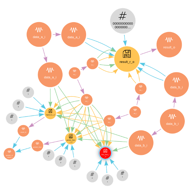
The graph structured database generated from Amida’s parsing of the RTL identifies data (wires, ports, constants, registers, and latches) and hierarchy (modules) as Nodes and the associated transforms, conversions, and manipulations of that data (conditional statements, assignment equations, procedural elements, and synchronous operations) as Edges. An example graph structure is shown in Figure 1. The primary goal of the graph is to identify and objectively measure the influence of any given element (Node or Edge) based on the fan-in, fan-out, distance to primary inputs and outputs, flow complexity, and other metrics.
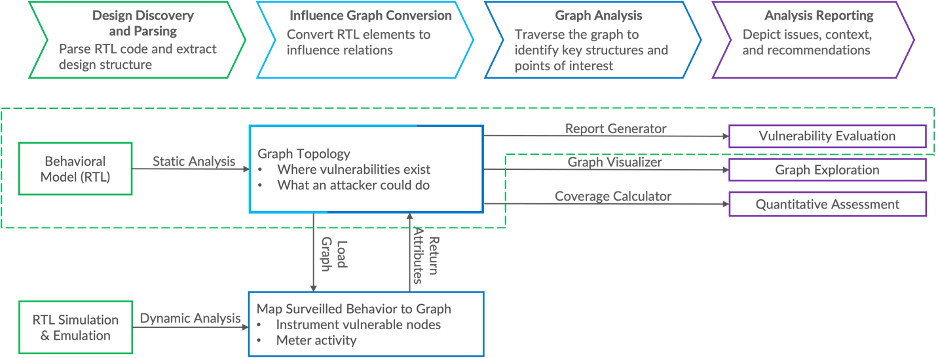
Influence statistics are fed to an algorithmic assessment that produces reproducible vulnerability scores associated with Nodes and Edges. The vulnerability locations within the graph trace back to specific lines or regions of code within the RTL model. In order to investigate certain topological features, we developed a native graph visualizer that captures complex RTL attributes and markings (e.g., the activity level of certain RTL elements, the physical distance between certain nodes or edges, etc.).
The primary purpose of the RTL-to-graph conversion and the subsequent graph visualization is to allow algorithms to predictively identify where to place attacks (exploiting a vulnerability) and where to place instrumentation for data collection (where to best observe an exploited vulnerability). The data collected from normal operation (simulation or emulation of the device in design) is fed, as a training set, to a patented machine learning tool that can identify and detect and attacks. These data are used to optimize – in a “transfer learning” sense – the instrument type and placement and can be used to quantitatively assess the hardening process. The ultimate outcome of this enhancement is a quantitative assessment of the “susceptibility of the attack surface” and the concomitant “risk of exposure to specific types of attack”.
Methodologies and Practices
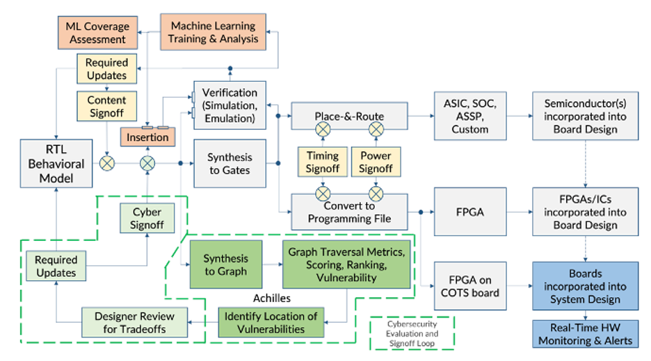
Amida’s methodology, shown in Figure 2, continuously evaluates the design model for exploitable vulnerabilities. This effort is similar to the design-for-X methodologies (testability, debug, manufacturing, etc.) and is known as Design-for-Security-and-Trust (DFST). DFST is a design methodology that comprises software tools, verification steps, and quantifiable metrics. It is applied through the periodic (e.g., weekly) behavioral model freeze. The cyber-signoff, shown in green in the picture below, identifies cybersecurity vulnerabilities. The routine application of functional operation vectors aligns to the assessment of dynamic evaluation of the various elements of the RTL model (it is a task that is already accomplished by the verification team, not the addition of a new methodology). When the design has been deemed complete (matches the specification), it should also complete the hardening process. The final hardened model is then sent through physical design where it must meet timing, testability, power, and other required signoff steps before the device can be sent to manufacturing (or implementation in the case of a programmable device).
AI Infrastructure and AI Software Development
The graph representation of converted RTL creates a novel database construct that can be used to identify the location of both vulnerabilities and instrumentation (detection, learning, and remediation). The instrumented RTL model can produce data that can be captured by machine learning parameters, and can also be used to measure the nominal behavior and anticipated duty cycle of each RTL element. During semiconductor device design or programmed model development, the machine learning model can be used to provide efficiency and coverage assessment of the instrumentation – which instruments contribute to the detection and identification results and how much they contribute. We have built such a system in prototype and demonstrated its efficacy as part of our SBIR Phase II work.
We recently received the industry’s first-ever patent for an in-silicon AI infrastructure that detects behavioral anomalies, identifies, and classifies the perturbation, and pinpoints its root cause. Our learning instruments observe the behavior from a pristine behavioral and deliberately infected) model. Attacks may represent behavior modifiers such as unauthorized take-overs, kill-switches, and alternate-functions; may represent reliability impacts such as accelerated-aging attacks, spoofed defects and faults, and destructive-operations; may represent infiltration-leakers such as code-injection and state-injection attacks; and may represent exfiltration-leakers such as critical data exposure and theft and proprietary structure exposure for reverse-engineering. We “teach” (train) the machine learning model through instruments and data collected from functional operations for all of these exploits.
Cyber-Supply Chain Risk Assessment (SCRM)
The Amida solution will produce semiconductor devices that contain cyber-hardened instrumentation. The instrumentation also includes root-of-trust identification (e.g., unique per chip ID numbers) that resides behind restricted access devices such as locks-and-keys or challenge-response features. Similarly, the per-chip IDs can be amalgamated at the system level. The same computer-based or hardware appliance-based device that conducts the machine learning training inherently includes the capability to identify ID’d instrumentation. In essence, hardening and root-of-trust instrumentation significantly enhances all aspects of the semiconductor and electronic sub-assembly supply chain.
These chips, when placed on boards provide an embedded cybersecurity infrastructure at the lowest level of the board design and can be integrated into a board-level access network such as a high-bandwidth 1149.1/1687 instrumentation architecture. Moreover, these protected chips enable intermediate retraining that can assess both the root-of-trust (verification that the devices are not counterfeit) and extend capability of instrumented CMCs to monitor cyber-malfeasance at the board-level.
When these boards are placed within the system, the device-embedded instruments can be extended to the system level, and the machine learning step provides a dedicated and optimized hardware appliance with the ability to produce both alerts and detailed diagnostic information to the device level. Attack indicators can be resolved to the device so the corrective actions can be accomplished at the lowest level (for example, if socketed, the chip may be changed, if not, the board containing the indicating chip may be swapped); if provided with embedded remediation, real-time corrective action can be activated. Attack data collected from instrumented systems can be stored and mined to track any trends in the supply chain (e.g., the attacked components all source from the same distributor, or were all manufactured in the same fabrication facility).
Cyber Analysis
Traditional coverage metrics only measure what is visible to a test bench or sandbox environment. Consequently, this figure-of-merit typically does not represent the physical characteristics of a device in the field, nor does it indicate how dangerous a subcomponent is in deployed operations. Code-coverage, for example, in the context of microelectronics, ensures that every line of code in the functional model (RTL) is exercised; unused code (representing unused features or functions) is revealed in relief and can represent (or be exploited by) vulnerabilities, back-doors, or malicious content. Fault-coverage – expressed as the ratio of the number of tested faults divided by the number of possible faults – assumes that the denominator is objectively discoverable, calculable, or known (and for cybersecurity analysis, achievable through the application of functional vectors, not test mode vectors). None of these are generally true when applied to cybersecurity.
There are formal methods, linters, and rule checker engines to discover instances of known (bad or dangerous) patterns in the RTL or gate level netlist, or track information to determine if key signals could be leaked or externally influenced. While helpful for direct investigations – and by no means do we advocate abandoning them – these approaches only allow us to quantify patterns that have been studied before; they are retrospective and after-the-fact evaluations that depend on prior descriptions (they are forensic in nature). In the context of quantitative threat assessment, those metrics choose their own denominator.
Amida’s approach connects static structural analysis to dynamic behavioral analysis of semiconductor devices to create a reproducible quantitative assessment of chip security. The outcome will be a numeric “vulnerability coverage.” We can simultaneously: identify the most likely place an attack will occur, the kind of intrusion that might occur there, and whether the element is exposed during normal operations (and using machine learning, is predictive). The static analysis indicates where exploitable vulnerabilities exist in the design; we have this already based on our prior work with the Navy. The dynamic analysis indicates how much an element is exercised during ordinary pre-silicon operational evaluation; combining them quantitatively determines a device’s overall vulnerability (exposure to risk per attack category as well as the overall combined susceptibility of all attack categories risk).
Our approach determines what elements of a device are most likely to be targeted by a bad actor. We can already determine where malicious inclusions such as kill switches, data leaks, unauthorized control, and catastrophic destruction would occur. The next step will be to identify structures, sites, and signals that should be scrutinized by designers and hardened against manipulation. Today we expand the aperture of the threat surface through a novel graph transformation that models the influence of internal elements on each other. Now, we want to produce a bouquet of objective metrics derived from our graph transformation. The main purposes of a quantitative measurement capability are to 1) produce a numeric value that can be used to differentiate good from bad; 2) to be able to use measurement values to steer hardening decisions; and 3) to be able to assess if a change (corrective action) has produced the required result (i.e., risk of exposure or attack has decreased).
The ultimate goal is to quantify the risk-versus-cost tradeoff in a way that illuminates the tradespace between remediation and resilience. We can already identify risks at a very fine level of granularity (per signal/structure in the RTL). And we can qualitatively assess the difficulty of implementing an intrusion versus the perceived value of that structure to an attacker. Now we need to objectively quantify it. No one has a repeatable method for doing this today. This is the problem we know how to solve.
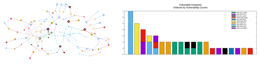
Our system identifies cybersecurity vulnerabilities into the behavioral model. The conversion of the RTL model to a structured graph produces transformed elements that more-easily reveal where attacks may occur, quantifies vulnerabilities to various attacks. For example, if there are 100,000 nodes in the graph that could be susceptible to kill-switch attacks and vulnerability analysis identifies 3,000 nodes, then that design has a susceptibility risk to kill-switch attacks of 3%. If the design is adjusted and the new modified design is converted to a graph and assessed again – and this time there are only 2,300 nodes, then the design has gone from 3% down to 2.3% susceptibility to kill-switch attacks. This is what we mean by a cybersecurity “coverage”. We provide both a qualitative assessment that can be used to drive cyber-hardening processes, as well as a quantitative measurement that determines “goodness” or a “risk assessment” level. Our approach combines the best features of code- and fault-coverage into a new category called vulnerability coverage.
The graph transform methodology exposes vulnerabilities that are currently undiscoverable by any commercial tool or formal method. Moreover, we can easily traverse the layers of model abstraction to create behavioral vectors – lines of application code analogous to fault pattern injection – that can exercise the vulnerability and actively determine whether it is physically present or not. This is an especially important breakthrough because latent hardware Trojans are mostly quiescent in structural test; they are only activated when the chip is in an operational state (except for a few cases of using test to expose design structures for reverse-engineering). This is, of course, our adversary’s objective and the primary purpose of the assessment.
There are two more collateral benefits. First, we can compactly instrument the most-valuable components whose manipulation would result in destructive or catastrophic outcomes; no other method can systematically identify where in the circuit topology a problem might occur and what the incursion would be. The physical protection of those elements is a design choice that is enabled by our technology. Moreover, if there were an escape – an unauthorized behavior detected by surveillance – those resources can be re-targeted to mitigation or in-situ repair.
Summary-Conclusions: Cybersecurity Assessment
A need for a quantitative measurement capability is well evidenced from Congresswoman McClain’s directive report language in the NDAA bill (HR 2670). It reads
“[a semiconductor begins] as a software program before it is fabricated, mostly in East Asia, into a chip. That software process is inherently vulnerable and a potential long-term threat to U.S. national security. Consequently, the U.S. defense industrial base has vulnerabilities that could be exploited.”
Her language refers to the National Security Agency’s Joint Federation Assurance Center Hardware Assurance Lab (July, 2022) report on “DoD Microelectronics: Levels of Assurance Definitions and Applications” that “characterizes the threats and risks to CMCs used in Department of Defense (DoD) systems.” Recognizing the threat, the guidance endeavors to assist programs with a better understanding of their system and components to effectively mitigate against threats. Per the NDAA language, Amida can:
- assess the security risk of threats and vulnerabilities to the Department of Defense in the software design component of semiconductor manufacturing acquisition
- support the Department of Defense, in creating a rigorous pre-production testing to detect the existence of and prevent the exploitation of design vulnerabilities
- support the Department of Defense in creating a comprehensive functional, structural, and behavioral analyses specifically designed to expose points of access that could be exploited for unauthorized manipulation prior to commitment to silicon
- assess the resources that would be required to execute points 2 and 3 above across the national security infrastructure
- assess the risk to continuity of operations and execution of national following a semiconductor supply chain attack at the software design level, creating the framework to address those risks
No end-to-end hardware security solution exists today to instrument and harden semiconductors for anomaly detection and attack remediation. Amida’s Design-for-Security-and-Trust (DFST) will fill this gap by automating semiconductor vulnerability assessment at scale as part of the design process, enabling cyber-hardened silicon through vulnerability analysis, and embedded instrumentation for on-going system monitoring.